
Introduction
5G is almost here! Many countries have already introduced 5G, while others are experimenting with it. 5G brings with itself a new set of challenges for the PCB industry. The old ways of manufacturing and production will not be enough. We will need more modern PCBs to support high-speed communication technology. As a result, PCBs are going to change considerably.
We have prepared this guide for the PCB manufacturers, hobbyists, and engineers. I will help you get an idea of the new PCB requirement for 5G. With the information, you can transform your PCB manufacturing process to suit 5G.
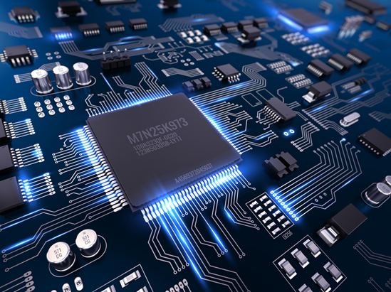
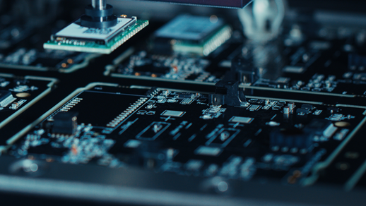
(High tech electronic PCB (Printed circuit board) with processor and microchips.)
How will 5G Impact the PCB Industry?
The 5G industry will need a high number of PCBs for functioning. As you know, the old methods of PCB manufacturing will not suffice. The PCB industry will have to prepare itself for the future.
5G will impact the PCB industry in many ways. First, it will have to deal with the small form factors of PCBs. The high traffic and data rate of 5G will also affect PCB manufacturing.
For this reason, most 5G PCBs will me multilayer PCBs.
5G will operate at much higher frequencies than 3G or 4G. As a result, the demand for high-frequency and complex PCBs will increase. PCBs for 5G will also need to be high-speed. So we may see an increased use of high-speed copper clad material. Apart from being high-speed, the PCBs will also depend on high-density.
Thermal management of PCBs will also be necessary for 5G applications. We may see PCB manufacturers using high thermal conductivity materials. They may even come up with an advanced heat-dissipating structure for PCBs. We may also see PCB manufacturers using non-traditional materials for more durability.
The whole PCB industry needs to adapt to meet the needs of 5G. It has already begun, and we are going to see the changes slowly.

(5G network wireless systems and internet of things with modern city skyline)
Next, a few words on PCB technology improvement for 5G.
How can the PCB Technology Improve?
PCB manufacturers will have to improve their technology to match 5G requirements. The old ways of manufacturing will not do. We will need more multilayer PCBs. Drilling will also acquire high importance for quality and reliability.
- The Need for Multilayer PCBs
5G will bring high rates of data transfer and traffic. It will increase the need for complex, high-performance PCBs. Naturally, standard PCBs will not be able to serve the purposes of 5G. Most PCBs for 5G will be hybrids using a multilayer construction.
Multilayer PCBs are small and able to fit the compact electronic equipment of 5G. They can offer more functionalities in a limited space. It’s also lightweight and ideal for modern smartphones, routers, and antennas.
Multilayer PCBs are also durable and can withstand high pressures. They also offer high connectivity and pack more capacity and speed.
PCB manufacturers will have to switch to multilayer PCB production for the 5G era.
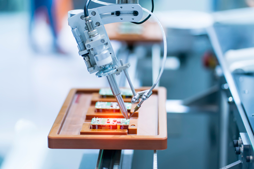
(robotic soldering used in soldering multilayer board and shielding case)
- Need for a Drill
You will need to use precise drilling process for 5G PCBs. Manufacturers use drilling to create holes on PCBs. The holes are then metalized to create vias. This way, the conductive layers form a connection with each other.
Improper drilling can lead to many drawbacks. You can encounter fractures, smearing, or burring.
Smearing can ruin a PCB beyond repair. Fractured PCBs become useless and are not fit for the application.
You will also need to be careful about the plated-through-hole (PTH) process. So drilling is a significant process of making 5G PCBs and requires careful consideration.
Now we will discuss the importance of laser marking for 5G PCBs.
In the PCB, how much do you know about Laser Marking?
Laser marking helps PCB manufacturers to label their circuit boards. You can use the process to put codes, marks, and other identifiable signs. The method of laser marking for 5G PCBs will be a little different.
- PCB Laser Marking Traceability
PCBs for 5G will be small and compact. They will need to establish data traceability for quality control. The laser marking will enable manufacturers to give ID information code to the PCBs. The PCB ID is useful for machine-reading during assembly. It is the first step to establishing data traceability.
You can also use laser marking to engrave-
- QR codes
- Labels
- Dates
- Drawings
Laser marking saves time and allows for more precision. The laser vaporizes the surface material of the PCB or changes its color. This way, a permanent mark is made. The process also involves low heat and creates no pollution. Laser marking is also easy to operate.
Laser marking will be a vital step to make PCBs for 5G applications.
- FPC Laser Cutting
FPC laser cutting is ideal for FPC and rigid-flex boards. You can also use the process for FR-4 PCBs. Laser cutting results in high precision and cleaner cutting edges. You can also cut tiny areas easily using FPC laser cutting.
The laser cuts the board without any touching or pressure. The contactless method helps prevent fractures and chipping. The process is also cost-effective and provides high efficiency. PCB manufacturers will need to change to FPC laser cutting to make 5G PCBs.
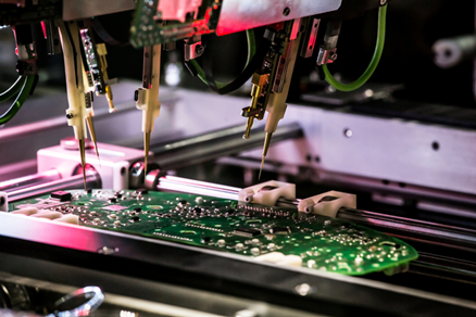
(Multi-purpose flying probe system for widest range of test requirements.)
In the next section, we will take a look at the advantages of laser cutting.
Learn about Advantages of Laser Cutting
Laser cutting provides a host of advantages over the traditional methods. It is ideal for complex and compact PCBs that you find in 5G equipment. Some of the benefits include-
- High precision: Laser cutting provides clean cuts matching your exact specifications.
- Fast:Laser cutting is much faster than manual or other cutting methods. You can cut multiple batches of PCBs in a short time.
- Ideal for small PCBs:Laser cutting can handle small PCBs. You can easily cut PCBs with small radius or sizes with high accuracy.
- Contactless:The whole process is contactless and doesn’t put any pressure on the PCB.
- Low heat:The cutting doesn’t produce any heat that can damage the PCB.
- Automatic positioning:The laser machine cuts the PCB automatically for the highest efficiency.
- Cost-effective: Laser cutting saves cost and time for higher profits.
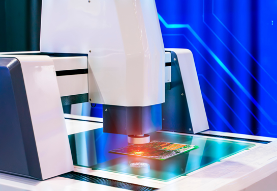
(Robotic vision sensor camera system in intellegence pcb factory)
Now we will discuss the importance of final plated finish for 5G-geared PCBs.
Why will the Final Plated Finish be More Important than Ever?
PCB manufacturers use a plated finish on their PCBs. The protective layer above the copper pcb conductor prevents oxidation and reliability issues. The plated finish is crucial to limit conductor losses. That’s why the plated finish is so vital to PCBs for 5G applications.
Manufacturers may use different materials to produce the plated finish. Silver and silver plating are excellent choices to provide the finishing touches. Silver is affordable and has a low melting point. It also has excellent thermal and electrical conductivity. It’s one of the best materials to use for PCB plated finish for 5G purposes.
You can also use palladium or platinum plating, and they are lighter and cheaper than gold. The high electrical conductivity of the materials also makes them the best choice for electroplating. Such plating enables PCBs to carry high currents and signals and limit distortions.
The plated finish impacts the performance and reliability of the PCB. So it’s highly crucial for PCBs made for 5G equipment.
(Close-up Macro Shot of Electronic Factory Machine at Work)
In the next part, we will cover the prominent uses of PCB in 5G technology.
The Top Use of PCBs in the 5G Era
The use of PCBs will increase considerably in the 5G era. We are going to see new and improved PCBs to handle big data and traffic needs of 5G. The top uses of PCB in 5G will be in the equipment and infrastructure.
5G base stations will need a large number of PCBs. 5G has a reduced coverage area than 4G and requires more power to make it up. Each 5G base station will need two times more PCBs compared to 4G stations. The 5G antennas will also need a considerable number of PCBs.
5G RF boards will require PCBs for functioning. The servers will also depend on PCBs for their operation. We will also find the use of PCBs in the motherboards of 5G equipment. In the same way, transmission devices and RF devices will also create a bug demand for PCBs.
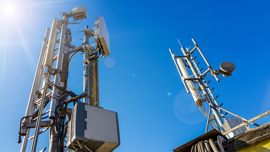
(5G smart mobile telephone radio network antenna base station)
Conclusion
PCB manufacturers need to be aware of the changes that technology brings. 5G will bring new standards for PCBs, and manufacturers need to adapt. You can easily prepare yourself for the future by reading our guide. If you have any more questions, you can get in touch with us.